Advanced Semiconductor and Packaging Technology
Master Packaging Technologies, Simulation Tools, and Advanced IC Design for Next-Gen Electronics
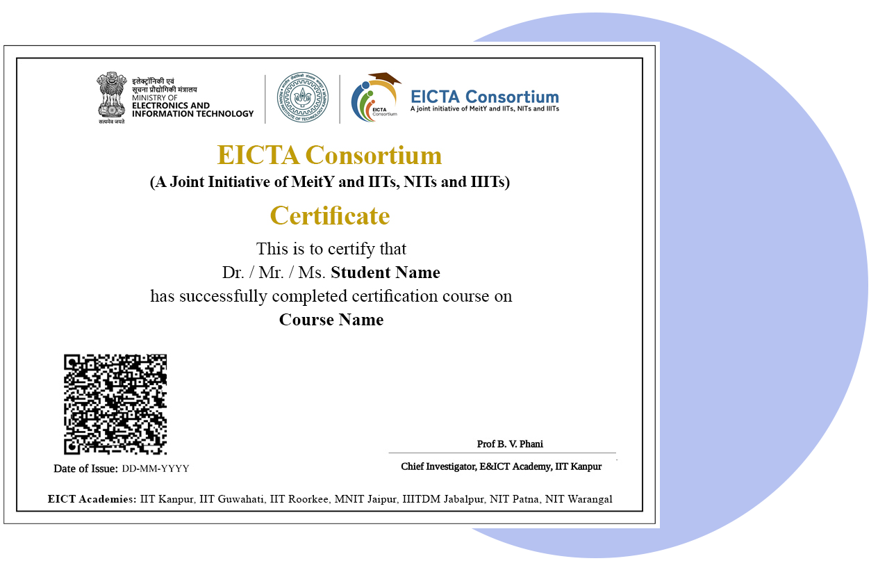
- Certificate from E&ICT Academy, IIT Kanpur upon successful course completion
- 40 hours of expert-led online live training and hands-on lab simulation
- Learn ANSYS, TCAD, and FEM tools through real-world packaging challenges
Faculty Development Program
Certification
Online Live
Interactive Instructor-Led Sessions
40 Hours
Course Duration
What you'll learn
- Understand the core principles and materials behind modern semiconductor packaging technologies
- Analyze thermal and electrical performance of IC packages using industry tools
- Simulate packaging behavior with FEM and TCAD software (e.g., ANSYS, Silvaco)
- Gain practical knowledge of 3D integration, fan-out packages, and co-packaged optics
- Learn to troubleshoot issues like underfill flow, fatigue failures, and thermal dissipation
- Bridge theoretical concepts with hands-on lab experiments and real-life engineering problems
Skills you'll gain
Semiconductor Packaging DesignThermal & Electrical SimulationTCAD-Based Device ModelingANSYS-FEM for Package TestingFailure Analysis & Reliability TestingAdvanced IC Interconnect TechnologiesHigh-Density Substrate EngineeringLab-Based Problem SolvingSystem-in-Package (SiP) and 3D IC TechniquesApplied Semiconductor Manufacturing Insights
Tools

Earn a career certificate
Add this credential to your LinkedIn profile, resume, or CV. Share it on social media and in your performance review.
Expert Faculty & Industry Mentors
Learn directly from top researchers and semiconductor design professionals with real-world experience.
Hands-On Simulation Experience
Apply concepts with TCAD, ANSYS, and FEM in lab-based scenarios for maximum practical exposure.
Industry-Relevant Curriculum
Covering the latest in 3D packaging, thermal modeling, co-packaged optics, and reliability engineering.